AMBER X
The unique analytical platform for large-volume sample characterization and maximum universality in sample preparation.
The unique analytical platform for large-volume sample characterization and maximum universality in sample preparation.
PRODUCT BROCHURE

AMBER X brochure
A unique combination of Plasma FIB-SEM. Download AMBER X brochure!
PDF – 6.1 MB
KEY FEATURES
Universality in sample imaging with field-free ultra-high resolution Optics
- - The BrightBeam™ SEM column delivers field-free ultra-high resolution imaging (0.9 nm at 15 keV, 1.3 nm at 1 keV) while maintaining universality in sample imaging and analysis.
- - Excellent imaging performance at low-beam energies ideal for imaging non-conducting samples and uncoated biological specimens. A low vacuum mode is also available.
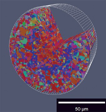
- High electron beam currents up to 400 nA are advantageous for microanalytical techniques such as CL, EDX, WDX and EBSD. - - Detection system with angle-selective and energy-filtering capabilities give complete control of surface sensitivity and the option to explore with different contrast.
Specification
| Electron Gun | High Brightness Schottky Emitter |
|---|---|
| Resolution | |
SE | 0.9 nm at 15 keV / 1.5 nm at 1 keV |
| Magnification | 2x - 2,000,000x |
| Accelerating Voltage | 50 eV to 30 keV |
| Probe Current | 2pA to 400nA |
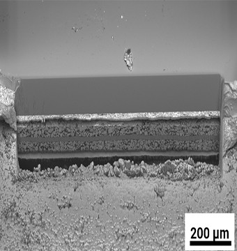
Extremely powerful Xe plasma FIB column
Xe plasma ion source FIB column for achieving the most challenging large-scale milling tasks in unbeatable short times frames
- - 50x faster than Ga LMIS FIBs.
- - on beam range current of 1 pA to 3 µA and resolution of < 12 nm
- - Newly developed high resolution Xe plasma FIB column achieving resolution of < 12 nm for extended patterning capabilities
- - Large-mass xenon ions with larger FIB current range for ultra-fast sputtering even without gas-assisted enhancement
- - Significant reduction in ion implantation compared to Ga LMIS FIBs
- - Rocking Stage - An effective and optimized polishing strategy against curtaining effect
Ion Optics
| Ion column | i-FIB + 1.5v | |
|---|---|---|
| Ion Gun | Xe plasma ion source | |
| Accelerating voltage | 3kV to 30kV | |
| Probe current | 1 pA to 3 µA | |
| Resolution (at 30 keV) | < 12 nm | |
Maximum Field of View | > 1 mm | |
| SEM-FIB angle | 55° | |
.jpg)
.jpg)
.jpg)
Application
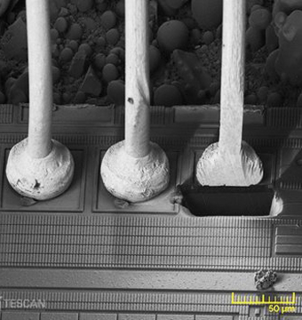
Semiconductors & Microelectronics
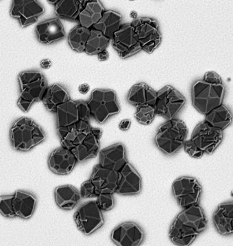
Material Science
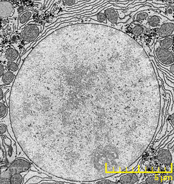
Life Sciences
Earth Sciences