SOLARIS
The most advanced capabilities in nanofabrication for ultimate quality in challenging sample preparation.
The most advanced capabilities in nanofabrication for ultimate quality in challenging sample preparation.
KEY FEATURES
Triglav™ - newly designed UHR electron column
- - TriLens™ - objective system: a unique combination of three-lens objective and crossover-free beam path
- - Advanced detection system with multiple SE and BSE detectors - TriSE™ and TriBE™
- - Triglav™ - Ultimate ultra-high resolution at low beam energy: 0.9 nm at 1 keV and 0.6 nm at 15 keV
- - Electron beam currents up to 400 nA and rapid beam energy changes
- - Optimized column geometry for accommodating large wafers up to 8”, 12”
Specification
| Electron Optics | |
|---|---|
| Electron Gun | High brightness Schottky emitter |
| Resolution | |
| Standard mode In-Beam SE | 0.6nm at 15keV |
Beam Deceleration Mode | 0.9 nm at 1 keV |
Magnification | 5 x - 1,000,000 x |
| Probe Current | 2 pA to 400 nA |
Orage™ FIB column
High-performance Ga FIB column for ultimate precision in nanoengineering.
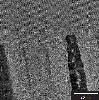
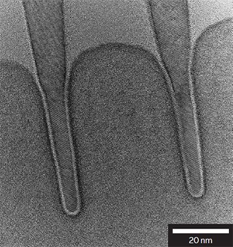
- Prepare high-quality, ultra-thin TEM lamella from the most advanced semiconductor nodes
- Easily obtain advanced geometry TEM lamella using optimized in-situ lift-out geometries and workflows
- AutoSlicer™ module for semi-automated FIB milling and TEM lamella preparation
- Gentle FIB thinning for improved quality results in TEM sample preparation
- Precise end-pointing at low kV for ultra-thin lamella preparation
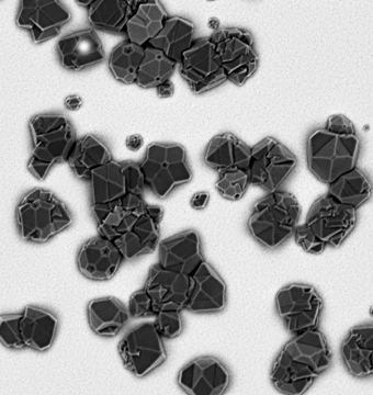
- Use low kV, ultra-high resolution imaging for beam sensitive materials or to generate high materials contrast
- Essence™ easy-to-use modular user interface
Ion Optics
| Ion column | Orage™ |
|---|---|
| Ion Gun | Ga LMIS |
| Resolution | <2.5 nm at 30 Kev (at SEM-FIB coincidence point) |
| Probe current | 1 pA to 100 nA |
| Accelerating Voltage | 0.5kV to 30kV |
SEM-FIB angle | 55° |
.jpg)
.jpg)
